
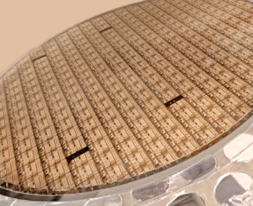
Arizona State University (ASU) and Deca Technologies (Deca), a provider of advanced wafer- and panel-level packaging technology, announced a groundbreaking collaboration to create North America’s first fan-out wafer-level packaging (FOWLP) research and development center. The new Center for Advanced Wafer-Level Packaging Applications and Development is set to catalyze innovation in the United States, expanding domestic…
CEA-Leti develops new gallium nitride/silicon process technology
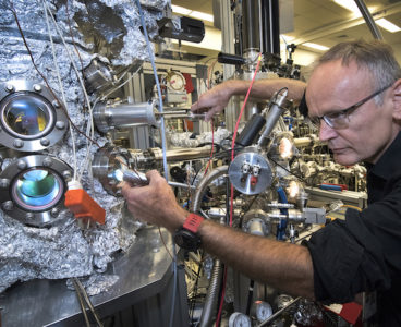
CEA-Leti has developed a 200 mm gallium nitride/silicon (GaN/Si) process technology compatible with complementary metal-oxide-semiconductor (CMOS) cleanrooms that preserves the high performance of the semiconductor material and costs less than existing GaN/SiC technology. In one of nine presentations at IEDM 2023, the institute said that current GaN high-electron-mobility-transistor (HEMT) technologies used in telecom or radar…
CHIPS R&D Chiplets Interfaces Technical Standards Workshop
The CHIPS Research and Development Office’s Chiplets Interfaces Technical Standards Workshop will be a hybrid in-person and virtual event from 8:30 a.m. to 5:30 p.m. EST, December 12, 2023, and 8:30 am to 12:30 pm December 13, 2023. The in-person event will take place at the NIST’s National Cybersecurity Center of Excellence (NCCoE) in Rockville,…
ACM Research’s new facility contributes to PNW’s growing semiconductor industry
ACM Research, a supplier of wafer processing solutions for semiconductor and advanced wafer-level packaging (WLP) applications, announces the grand opening of its new multi-use facility in Hillsboro, Oregon, on November 28. This is a first-of-its-kind property within North America for ACM Research, and its 11,000 ft2 will feature offices, warehouse space, and a dedicated cleanroom/demonstration…
Plasma-Therm announces acquisition of Thin Film Equipment
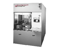
Plasma-Therm, a manufacturer of plasma-process equipment for the semiconductor and compound semiconductor markets, announces it has acquired Thin Film Equipment SrL (TFE), effective September 18, 2023. Based in Binasco (Milano, Italy), TFE is a supplier of sputtering equipment for semiconductor R&D and production and is well-known for its expertise in physical vapor deposition (PVD) sputtering and…
Three top foundries join Imec’s SSTS program

Imec, a research and innovation hub in nanoelectronics and digital technologies, has announced that GlobalFoundries, Samsung Electronics, and TSMC have joined imec’s Sustainable Semiconductor Technologies & Systems (SSTS) research program. Launched in 2021, the SSTS program rallies stakeholders from across the semiconductor industry – including systems companies, (equipment) suppliers, and now also three of the…
Rapidus, Japan’s new chip manufacturer, joins imec’s Core Partner Program
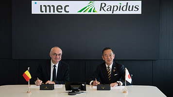
Imec, a global research and innovation hub in nanoelectronics and digital technologies, and Rapidus, Japan’s newly founded chip manufacturer, announced that they have taken an important next step in setting up a long-term and sustainable collaboration in the domain of advanced semiconductor research, with Rapidus joining imec’s Core Partner Program. During a Belgian economic delegation…
Electroninks uses Citrine Informatics’ AI-assisted R&D to develop enhanced silver ink
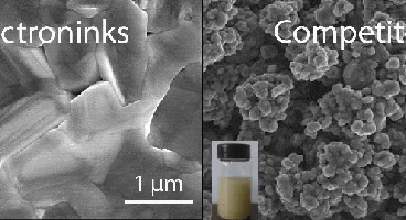
Electroninks, a maker of particle-free conductive metal inks and advanced materials, announces a redevelopment of their signature particle-free silver ink for aerosol jet printing applications enabled by Citrine Informatics’ AI-guided R&D platform. “Citrine’s groundbreaking AI-assisted software platform will help enhance not only our silver ink, but eventually all of our particle-free inks for new and…
Ohio grows into a globally recognized R&D hub

By Gordon Feller With top-notch universities, federal research institutes, leading companies from nine major industry sectors, and 14 top-ranked hospital systems, Ohio is a “quiet giant” of innovation in industrial sectors and life science. Ohio has the fifth-highest number of Fortune 500 and Fortune 1000 companies — and is home to more than 120 NYSE/Nasdaq…
‘Self-driving’ lab speeds up research, synthesis of energy materials
By Milad Abolhasani, NCSU and Matt Shipman, NCSU Researchers from North Carolina State University and the University at Buffalo have developed and demonstrated a ‘self-driving lab’ that uses artificial intelligence (AI) and fluidic systems to advance our understanding of metal halide perovskite (MHP) nanocrystals. This self-driving lab can also be used to investigate a broad…
Record-breaking, ultrafast devices step to protecting the grid from EMPs
From Sandia National Laboratories Scientists from Sandia National Laboratories have announced a tiny, electronic device that can shunt excess electricity within a few billionths of a second while operating at a record-breaking 6,400 volts — a significant step towards protecting the nation’s electric grid from an electromagnetic pulse. The team published the fabrication and testing…
Surprising semiconductor properties revealed with innovative new method

By Karyn Hede, PNNL A research team probing the properties of a semiconductor combined with a novel thin oxide film have observed a surprising new source of conductivity from oxygen atoms trapped inside. Scott Chambers, a materials scientist at the Department of Energy’s Pacific Northwest National Laboratory, reported the team’s discovery at the Spring 2022…
Thermo Scientific Centrios HX offers precise circuit edit solution for fast prototyping
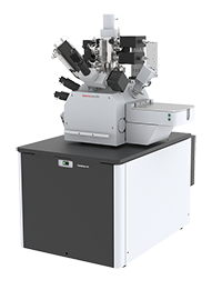
Thermo Fisher Scientific introduces the Thermo Scientific Centrios HX Circuit Edit System. This state-of-the-art circuit edit solution allows semiconductor manufacturers to optimize success rates with high resolution imaging and precise editing of today’s leading-edge devices. As semiconductor devices become more complex, higher precision circuit edit tools are required to optimize product functionality and deliver prototypes…
Inflation will be R&D game changer in 2022, in this week’s R&D power index

The R&D World Index (RDWI) for the week ending February 11, 2022, closed at 5,188.11 for the 25 companies in the RDWI. The Index was down -4.28% (or 231.98 basis points) from the week ending February 4, 2022. The stock of eight RDWI members gained value from 0.02% (Alibaba) to 5.34% (Daimler AG). The stock…
R&D 100 winner of the day: Ubiquitous Water Wand (UWAW)
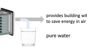
Ubiquitous Water Wand (UWAW), developed by Industrial Technology Research Institute (ITRI) and Chyi Ding Technologies, is an ultrahigh efficiency vapor/air separation equipment which extracts clean water from the air we breathe. It provides ultra clean drinking water without water sources, cooling media or water filters. In conjunction with an air-conditioner, UWAW can also provide buildings…
Rising inflation rates undermine economic growth, in this week’s R&D Power Index
The R&D World Index (RDWI) for the week ending January 21, 2022, closed at 5,208.27 for the 25 companies in the RDWI. The Index was down -5.66% (or 312.43 basis points) from the week ending January 14, 2022. The stock of only one RDWI member gained value at 0.42% (AstraZeneca). The stock of 24 RDWI…
R&D increasing in new fields despite rising inflation, in this week’s R&D Power Index
The R&D World Index (RDWI) for the week ending January 14, 2022, closed at 5,520.70 for the 25 companies in the RDWI. The Index was up 0.89% (or 48.45 basis points) from the week ending January 7, 2022. The stock of 18 RDWI members gained value from 0.03% (Facebook) to 5.11% (Toyota Motor). The stock…
New technology takes users from quantum dot to manufacturing in less than an hour
Artificial Chemist 2.0 is a new technology that allows users to go from requesting a custom quantum dot to completing the relevant R&D and beginning manufacturing in less than an hour. The technology is completely autonomous and uses artificial intelligence (AI) and automated robotic systems to perform multi-step chemical synthesis and analysis. Quantum dots are…
R&D winner of the day: Superconducting MgB2 wire for high-efficiency electromagnets
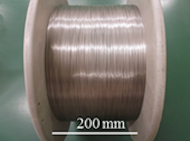
Hitachi has developed a superconducting 8-km-long magnesium diboride (MgB2) wire for high-efficiency superconducting electromagnets. This superconducting wire not only reduces the cooling power of the magnets for the klystron but also contributes to the energy saving of existing superconducting devices such as MRIs. It will also contribute to environmental load reduction as its application is…
Materials – Turning down the heat
By Karen K Dunlap Scientists at Oak Ridge National Laboratory and the University of Tennessee designed and demonstrated a method to make carbon-based materials that can be used as electrodes compatible with a specific semiconductor circuitry. The work bridges nanoscale 3D printing and widely available processes for complementary metal-oxide-semiconductor, or CMOS, technologies to enable biosensors…
Dance, electron, dance: Scientists use light to choreograph electronic motion in 2D materials
By Theresa Duque A team of scientists led by the Department of Energy’s Lawrence Berkeley National Laboratory (Berkeley Lab) and UC Berkeley has demonstrated a powerful new technique that uses light to measure how electrons move and interact within materials. With this technique, the researchers observed exotic states of matter in stacks of atomically thin…
One new valve — and three reasons it could change semiconductor manufacturing
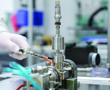
By Matt Ferraro, Product Manager, Semiconductor The semiconductor market is not an easy one to navigate. Semiconductor wafer fabricators are under constant pressure to maintain maximum precision in highly complex processes that involve expensive materials, corrosive gases, and extreme temperatures. There is little room for error, especially given the added strain of keeping up with…
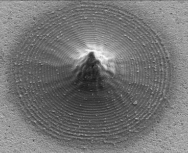
Electrons, not ions, provide superior plasma etching of nanoscale semiconductor devices
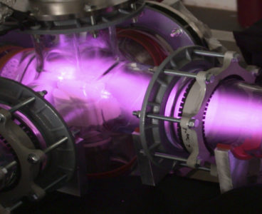
In semiconductor fabrication, the traditional approach to dry etching has been to utilize RF plasma to bombard the surface of the wafer with positive ions to remove material between masking layers. Although ion etching has been effective for decades, it fails to produce the precise, sharp, nano-sized structures and pathways required in next generation devices. …
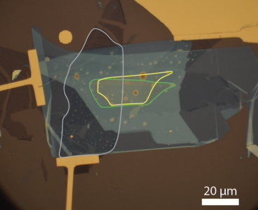
Making high-temperature superconductivity disappear to understand its origin
When there are several processes going on at once, establishing cause-and-effect relationships is difficult. This scenario holds true for a class of high-temperature superconductors known as the cuprates. Discovered nearly 35 years ago, these copper-oxygen compounds can conduct electricity without resistance under certain conditions. They must be chemically modified (“doped”) with additional atoms that introduce…
Reorganizing a computer chip: Transistors can now both process and store information
A computer chip processes and stores information using two different devices. If engineers could combine these devices into one or put them next to each other, then there would be more space on a chip, making it faster and more powerful. Purdue University engineers have developed a way that the millions of tiny switches used…